Photonic processors: light instead of electrons changes the rules of the game in data centers
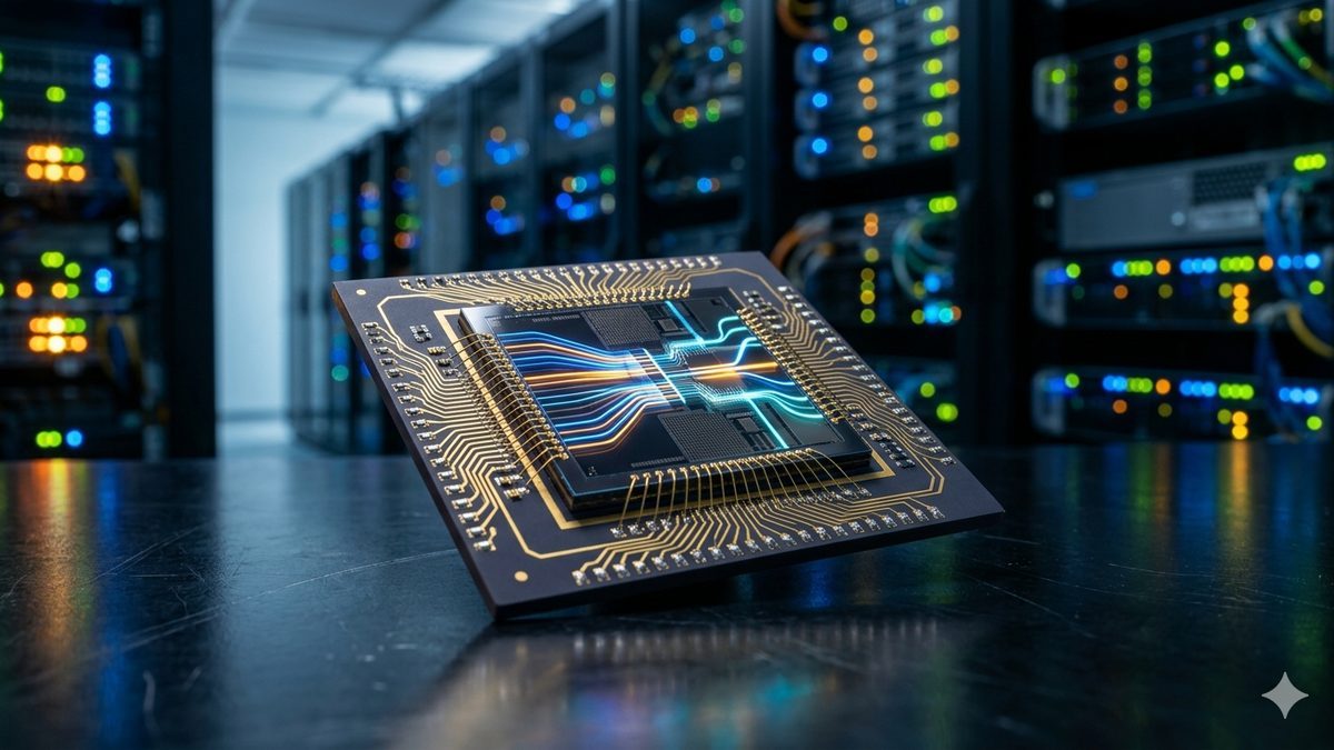
Photonic processors, which compute using light instead of electrons, are moving from the lab into commercial deployment. Companies such as Lightmatter, Ayar Labs, and Celestial AI (acquired by Marvell for up to $5.5 billion) are achieving order-of-magnitude lower energy consumption and higher data-transfer rates, but still face challenges in memory, precision, and nonlinear operations. The first commercial products are expected in 2027–2028.
Energy consumption in data centers is growing so fast that, according to the International Energy Agency, it will more than double by 2030 to roughly 945 TWh per year — as much as all of Japan consumes today. In advanced economies, data centers will be responsible for more than 20% of all growth in electricity demand. Meanwhile, today's chips are running into physical limits — heat, the resistance of copper interconnects, losses from charging and discharging transistor capacitances. The answer could be processors that compute with light. Photonic chips underwent breakthrough development in 2024–2026 and, for the first time in history, left the laboratories on their way to commercial products.
This is not a distant vision. Lightmatter unveiled the Passage M1000 — a photonic superchip offering 114 Tbps of optical bandwidth on a 3D photonic interposer spanning over 4,000 mm². Broadcom is shipping the Tomahawk 6 "Davisson," the industry's first 102.4 Tbps Ethernet switch with integrated co-packaged optics, using TSMC's COUPE packaging technology. And in December 2025, Marvell announced the acquisition of the startup Celestial AI — a transaction with a minimum value of $3.25 billion, which could rise as high as $5.5 billion upon reaching market milestones. It is to date the largest transaction in the photonic computing sector.
This article maps the current state of the technology, its physical principles, the key players, the real-world results, and the obstacles that have held it back so far.
Electronic processors compute by switching transistors — each switch means charging and discharging capacitances, that is, energy lost as heat. Photons behave fundamentally differently. They travel through waveguides with practically no resistive losses, do not need to charge any capacitances, and — crucially — can overlap in a single waveguide across dozens of different wavelengths without interfering with one another. This property, called wavelength-division multiplexing (WDM), enables massive parallelism without a proportional increase in physical components.
The basic building block of most photonic processors is the Mach-Zehnder interferometer (MZI) — a structure that splits an input optical signal into two arms, applies programmable phase shifts, and recombines the signals. The interference between the arms determines the output amplitude and phase, so an MZI implements a programmable 2×2 matrix transformation. A key mathematical insight (Reck et al., 1994) showed that any unitary matrix of any size can be decomposed into a cascade of such 2×2 transformations. Combined with singular value decomposition (SVD), this means that networks of MZIs can implement arbitrary matrix multiplication — the operation that dominates neural-network computation.
The landmark demonstration came in 2017, when a team from MIT (Shen et al., Nature Photonics) demonstrated a programmable photonic processor based on a cascade of MZIs performing vowel recognition — work that kicked off the modern era of photonic computing.
The second important building element is micro-ring resonators (MRRs), which, at resonance, selectively pass or block specific wavelengths. The "broadcast-and-weight" architecture uses banks of MRRs as programmable synapses — each input neuron transmits at a different wavelength, and the resonators on the output side set the weights for each channel.
The vast majority of current photonic processors function as hybrid electronic-photonic systems: the linear operations (matrix multiplication) are performed by the optics, while the nonlinear activations, memory, and control remain electronic. Fully optical processors are still largely experimental — photons hardly interact with one another, which makes it difficult to implement nonlinear functions purely optically.
Lightmatter, founded in 2017 as a spin-off from MIT, reached a valuation of $4.4 billion in October 2024 after a Series D round led by T. Rowe Price, with total funding of over $850 million. The company is the most visible player in the sector and works on two fronts: photonic computation and optical interconnects.
In April 2025, Lightmatter published in Nature the first demonstration of a photonic AI accelerator capable of running standard neural networks. The Envise processor integrates six chips in a single 3D package — four 128×128 photonic tensor cores and two 12 nm digital control circuits. The whole contains roughly 50 billion transistors and a million photonic components, achieves 65.5 TOPS (trillions of operations per second in the adaptive block floating-point format ABFP16) at a total power consumption of approximately 80 watts (78 W electrical + 1.6 W optical). On this hardware, unmodified ResNet and BERT models ran successfully with accuracy approaching that of 32-bit digital accelerators.
In parallel, Lightmatter is collaborating with GlobalFoundries on manufacturing the Passage product line for optical interconnects. In March 2025, the company unveiled the Passage M1000 (3D photonic interposer, 114 Tbps) and Passage L200 (3D co-packaged optics, 32–64 Tbps). In March 2026, the company extended its roadmap with the Passage L20 — a unified optical engine for NPO (Near-Package Optics) and OBO (On-Board Optics) applications with 6.4 Tbps in each direction, with sampling planned for the end of 2026.
In March 2026, Ayar Labs raised $500 million in a Series E round led by Neuberger Berman, with total funding of $870 million and a valuation of $3.75 billion. The company manufactures TeraPHY optical I/O chiplets that replace copper interconnects between chips and use TSMC COUPE technology. Its strategic investors are AMD and NVIDIA; Intel invested in earlier rounds as well. MediaTek, Alchip Technologies, and the Qatar Investment Authority also joined — a signal that the entire industry regards optical I/O as critical infrastructure. The company plans to ramp up high-volume production for AI systems deployed from 2028.
Celestial AI developed its Photonic Fabric technology with an optical interconnect that, according to the company's claims, achieves 25× greater bandwidth at 10× lower latency compared to conventional co-packaged optics solutions. Unlike ordinary CPO, which brings optically encoded data only to the edge of the chip, Photonic Fabric reportedly makes it possible to deliver data to any location on the processor.
In December 2025, Marvell announced the acquisition for at least $3.25 billion in cash and stock. If Celestial AI reaches cumulative revenues of $2 billion by the end of Marvell's fiscal year 2029, the total price could rise as high as $5.5 billion. The acquisition was completed in February 2026. Marvell expects revenue from Celestial AI technology starting in the second half of fiscal year 2028, with an annual run-rate of $500 million by the end of FQ4 FY2028 and $1 billion by the end of FQ4 FY2029.
In October 2025, Broadcom began shipping the Tomahawk 6 "Davisson," the industry's first 102.4 Tbps Ethernet switch with co-packaged optics — the third generation of Broadcom's CPO platform. The switch heterogeneously integrates optical engines based on TSMC COUPE technology with advanced packaging on the substrate, which according to Broadcom reduces the power consumption of the optical interconnects by approximately 70% compared to traditional pluggable optical modules.
At GTC 2025 (March 2025), NVIDIA announced the Quantum-X Photonics and Spectrum-X Photonics switches using TSMC COUPE packaging technology, aimed at interconnecting millions of GPUs in AI factories. In March 2026, NVIDIA invested $4 billion in laser manufacturers Lumentum and Coherent ($2 billion each) to expand silicon photonics manufacturing capacity.
Intel is continuing its Intel Silicon Photonics program with prototype optical I/O chiplets.
A Chinese team from Tsinghua published in Science in 2024 the Taichi photonic chiplet achieving 160 TOPS/W — and that on an older 180 nm CMOS process. Another Chinese team (Shanghai Jiao Tong University and Tsinghua) unveiled the fully optical LightGen chip with more than 2 million photonic "neurons," which according to its authors outperforms NVIDIA GPUs by up to 100× on certain narrowly defined tasks (image generation, denoising) — though it must be emphasized that these are specialized analog machines for specific tasks, not general-purpose replacements for GPUs.
Geopolitically, this is significant: silicon photonics is becoming a new front in U.S.-Chinese technological competition. Photonic computing does not require the most advanced lithography and opens an alternative path to competitive AI hardware beyond the reach of Western export restrictions on advanced EUV lithography.
iPronics has commercialized the programmable photonic processor SmartLight. The German company Q.ANT unveiled the NPU Gen 2, claiming markedly lower power consumption and higher performance for AI/HPC tasks compared to the previous generation.
Energy efficiency is the main argument for photonics. The ACCEL chip from Tsinghua University achieved a system energy efficiency of 74.8 POPS/W (peta-operations per second per watt) with a computational speed of 4.6 POPS — according to Nature (2023), this is more than three orders of magnitude (>1000×) better efficiency than state-of-the-art digital processors. It must be added, however, that ACCEL is a specialized analog chip for visual tasks (99% of the computation is performed optically), not a general-purpose processor.
In interconnects, co-packaged optics reduces consumption from roughly 15 pJ/bit (pluggable modules) to under 5 pJ/bit. Lightmatter measured an overall efficiency of 4.6 pJ/bit on the Passage platform (2.6 pJ/bit for photonics + laser, ~2 pJ/bit for SerDes).
In 2024, MIT demonstrated a photonic processor capable of ultrafast AI computations — image classification on the order of hundreds of picoseconds. Nature published the integrated large-scale photonic accelerator Lightelligence PACE, solving 64×64 matrix operations with latency on the order of nanoseconds.
Quantum computers also make use of photonics — with a different goal, but on the same material platform.
In February 2025, PsiQuantum published in Nature a manufacturing platform for photonic quantum computers — the Omega chipset designed for quantum computers with millions of qubits. The chips are manufactured by GlobalFoundries on standard 300 mm silicon wafers. The measured fidelities include 99.98% for single-qubit preparation and measurement, 99.5% visibility of two-photon quantum interference, 99.72% fidelity of the chip-to-chip quantum interconnect, and 99.22% for two-qubit fusion gates. PsiQuantum has raised over $2 billion in total and is building quantum computing centers in Brisbane (Australia) and Chicago (USA).
In January 2025, Xanadu unveiled Aurora — the first networked, modular photonic quantum computer. The system consists of 4 interconnected server racks containing 35 photonic chips and 13 km of optical fiber, all operating at room temperature. Aurora is a 12-qubit machine whose architecture is in principle scalable to thousands of racks and millions of qubits. The results were published in Nature. In November 2025, Xanadu announced a SPAC merger with Crane Harbor Acquisition Corp. with a pre-money valuation of $3 billion (combined entity ~$3.6 billion). Upon completion (a shareholder vote planned for March 19, 2026), it will become the first publicly listed pure-play photonic quantum company on NASDAQ and the Toronto Stock Exchange.
These two approaches — classical photonics for AI and quantum photonics for fundamentally different problems — are complementary. Classical photonic processors are closer to commercialization (2027–2028); quantum ones are targeting fault-tolerant systems around 2029 and later.
Lightmatter CEO Nick Harris openly admits that developing a scalable DRAM-type memory solution for photonics remains an unsolved challenge with no clear solutions. Whereas electronically writing a single bit costs on the order of single-digit femtojoules, photonic memory prototypes require on the order of thousands of femtojoules — that is, roughly a thousandfold worse efficiency. As Harris summarized it: even if you had a processor with zero power consumption and infinite speed, you would not gain even a twofold speedup, because the machine spends most of its time waiting for data.
The analog nature of optical processing means that the native precision is typically 4–8 bits, limited by noise, manufacturing variations, and thermal drift. Hybrid solutions such as bit-slicing can achieve higher effective precision by decomposing into multiple low-precision operations, but at the cost of losing the throughput and energy advantages. For training neural networks, which requires 16+ bits, this is still insufficient. Lightmatter nevertheless demonstrated that for inference with the ABFP16 format it achieves accuracy approaching that of 32-bit digital accelerators.
Photons hardly interact with one another, which makes it difficult to implement nonlinear activation functions purely optically. Current solutions require conversion into electronics for every nonlinear operation (ReLU, sigmoid), thereby introducing latency and an energy penalty. Emerging approaches such as acousto-optic activations help, but remain at the laboratory stage.
Silicon photonics brings new testing challenges — yield is still lower than for CMOS electronics, testing requires active thermal management and sub-micron fiber-alignment precision. Lightmatter addresses this problem with technologies such as vClick (surface fiber attachment enabling wafer-level testing) and eClick (attachment via the edge of the chip). The roadmap for the next generation of silicon photonics focuses on the heterogeneous integration of III-V lasers and improving yield.
The consensus of industry and academia agrees on a gradual, not sudden, transition.
Optical interconnects are already a commercial reality in 2025–2026. Broadcom is shipping CPO switches (TH6 Davisson), Lightmatter is sampling the M1000 and L200/L20, Ayar Labs is scaling TeraPHY production, and NVIDIA is investing billions in laser manufacturers for silicon photonics.
Photonic computing processors for AI inference should, according to analysts at Yole Group, be commercially shipping in the 2027–2028 period.
The silicon photonics market is growing at a rate of over 25–30% per year (CAGR) according to various analyst firms. Overall investment in photonics is accelerating sharply: the U.S. CHIPS Act, the European Chips Act, and direct strategic investments by tech giants (NVIDIA into Lumentum and Coherent, Marvell's acquisition of Celestial AI) signal that photonics has ceased to be a fringe technology.
A direct comparison with NVIDIA GPUs shows a nuanced picture.
For specific operations, photonic processors already demonstrate order-of-magnitude advantages. Photonic accelerators solve matrix operations with ultra-low latency on the order of nanoseconds, representing an order-of-magnitude speedup over electronic circuits for selected tasks. ACCEL from Tsinghua showed a more than thousandfold energy advantage over GPUs for visual classification, albeit only for narrowly defined tasks.
For general-purpose AI training, however, photonic processors cannot compete for the foreseeable future. NVIDIA offers the massive CUDA software ecosystem, terabytes of unified memory, and precision sufficient for training. Photonic processors have no equivalent to CUDA, have no memory, and their native precision is insufficient for training.
The most realistic path to competition is indirect: photonic interconnects can dramatically increase the efficiency of GPU clusters by removing bandwidth bottlenecks. Celestial AI claims 6.2 pJ/bit for memory transactions versus tens of pJ for conventional solutions.
For AI inference, the outlook is more favorable. Matrix multiplication dominates inference workloads, the trend of model quantization (FP8, INT4) converges with the precision of photonics, and sub-nanosecond latencies are attractive for real-time applications. Lightmatter demonstrated on the Envise chip that photonic processors achieve performance comparable to purely electronic counterparts at substantially lower power consumption.
Photonic processors represent the most promising architectural alternative to electronic chips since the introduction of GPU accelerators. Breakthrough publications in Nature in 2024–2025 confirmed that optical matrix multiplication achieves accuracy comparable to digital systems at orders-of-magnitude lower energy consumption.
Three critical shifts define the current state. First, Broadcom and NVIDIA are genuinely shipping and deploying CPO switches into production. Second, Lightmatter demonstrated the running of standard AI models on a photonic processor and published the results in Nature. Third, massive acquisitions and investments (Marvell/Celestial AI for $3.25–5.5 billion, NVIDIA's $4 billion into laser manufacturers, Ayar Labs' Series E of $500 million) signal that the major players consider photonics strategically essential.
Nevertheless, fundamental barriers remain — the absence of optical RAM, limited precision, and the need for conversion for nonlinear operations. Photonic processors will not replace GPUs in the foreseeable future, but will complement them: primarily as optical interconnects accelerating communication within GPU clusters, secondarily as specialized inference accelerators.
Realistically, the current state of photonic computing is comparable to where GPU accelerators were around 2007–2010 — the technology has proven its viability, the first products exist, but the ecosystem is only just maturing. Photonics is entering the mainstream through the "door of interconnects," not the "door of computation." Computing applications will follow.
Main sources: IEA "Energy and AI" report (April 2025); Nature: Lightmatter "Universal photonic artificial intelligence acceleration" (April 2025), PsiQuantum Omega chipset (February 2025), Xanadu Aurora (January 2025), Tsinghua ACCEL (2023), Tsinghua Taichi (Science, 2024); Broadcom TH6 Davisson press release (October 2025); Marvell/Celestial AI SEC filings and press releases (December 2025, February 2026); Ayar Labs Series E announcement (March 2026); Lightmatter Passage L20 announcement (March 2026); Xanadu SPAC filing SEC (November 2025); ServeTheHome, The Register, Data Center Dynamics, Optics & Photonics News; analyst estimates from Yole Group and MarketsandMarkets.
Article verified and updated as of March 11, 2026. For corporate performance claims that have not been independently reviewed, this is explicitly stated.
Creation transparency
The concept, structure, and editorial line of the article are the work of the author, who prepared the content outline, established the key theses, and directed the entire creation process. Generative AI (Claude Opus 4.6, Anthropic) was used as a tool for research, fact-checking, and fleshing out the author's draft.
The author verified the key findings and approved the final wording. No part of the text was published without conscious authorial control. The factual data were verified against the publicly available sources cited in the text.
The procedure complies with the transparency principles of EU Regulation 2024/1689 (AI Act). #poweredByAI
Read the Czech original on Médium.cz.
AI · Claude — machine translation, may contain inaccuracies.